搜索内容
登录
首页
活动
研讨会
论坛
专栏
技术子站
学院
试用
头条
更多
兆威机电发布机器人灵巧手重磅新品!单板控制,17个自由度,寿命大于10年
第一批新能源车主换电池:“25万买车,12万换电池”“费用高过汽车残值”
卫星通信产业爆发前夕:IoT-NTN率先商业化、国产芯片厂商出招解决成本挑战
ADI收购了一家eFPGA公司,可重构芯片成为FPGA发展新风向?
宁德时代全固态电池开启样品验证,能源新世纪即将到来
储能变流器中的“蓄水池+滤水器”——薄膜电容
拓展AI数据中心内存,第二代AMD Versal Premium系列自适应SoC,首发支持CXL 3.1、 PCIe Gen6
今日看点丨消息称三星正考虑委托台积电量产 Exynos 芯片;LGD开发出可穿在身上的拉伸显示屏
工商业储能逆变器正密集发布
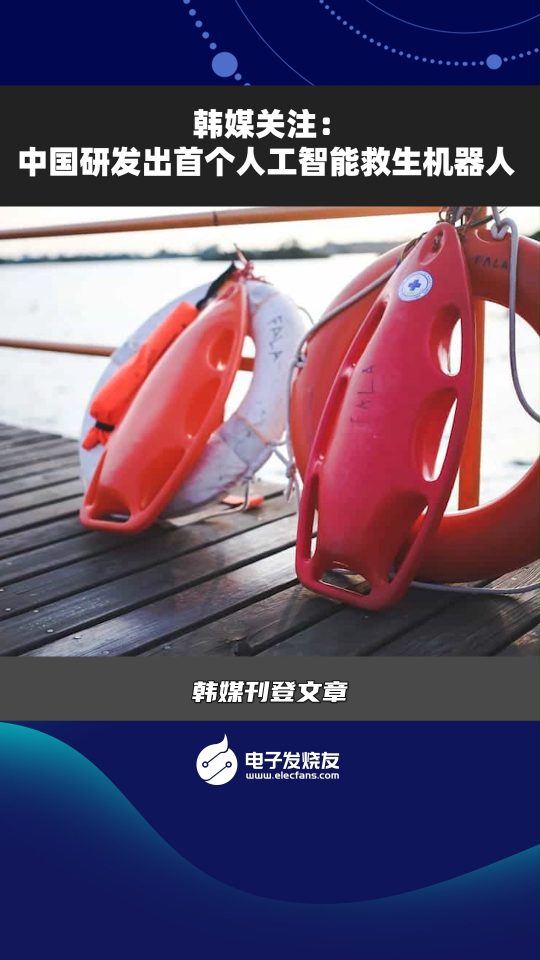
韩媒关注:中国研发出首个人工智能救生机器人
曾毓群:若特朗普“开绿灯”宁德时代将考虑赴美建厂
2024年可穿戴设备产业市场和热点技术解析(下)
2024电机控制先进技术研讨会
研讨会
直播
更多
28
11月
功率表的基础知识及其校准
2024/11/28 10:00-11:30
9779
去报名
17
10月
Sunlord产品在AI服务器中的应用
2024/10/17 10:00-11:30
66987
去观看
25
09月
元器件阻抗测试的完整解决方案
2024/09/25 10:00-11:30
61907
去观看
OpenHarmony板级移植:RK3568移植分享
2024/11/14 19:00-20:08
1.7万
去观看
数据智能系列讲座第4期:预训练的基础模型下的持续学习
2024/10/30 20:00-21:18
2.1万
去观看
2024开放原子开源生态大会——开鸿助力产业生态与人才培养分论坛
2024/09/26 13:30-17:21
1.1万
去观看
专题
更多
2024电机驱动和控制前沿观察
万物智联,共AI共腾飞
技术迭代加速,可穿戴迎来创新发展新动能
新品快讯
更多
· Microchip推出广泛的IGBT 7 功率器件组合, 专为可持续发展、电动出行和数据中心应用而优化设计
· 英飞凌推出新型高性能微控制器AURIX™ TC4Dx
· Rambus宣布推出业界首款HBM4控制器IP,加速下一代AI工作负载
· 华邦电子推出全新LPDDR4/4X,打造汽车行业的绿色解决方案
· 安森美推出业界领先的模拟和混合信号平台
推荐
电子发烧友网官方
韩媒关注:中国研发出首个人工智能救生机器人
昨天
恩智浦MCU加油站
专栏
恩智浦FRDM-MCXA153 RT-Thread实践指南 实现和优化RT-Thread的SPI驱动
昨天08:58
英飞科特电子
�


 搜索内容
搜索内容


 韩媒关注:中国研发出首个人工智能救生机器人

 9779
9779